xxx
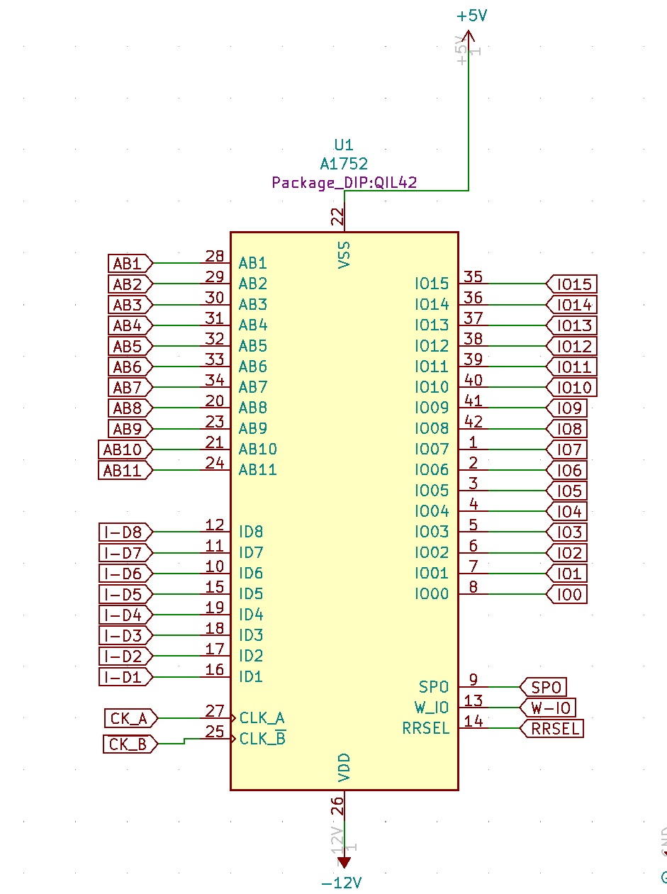
A17xx is a Memory & IO circuit. It has 3 different functionalities. It contains 1x16 I/Os manager and 2 memory blocks. Memory blocks are:
This circuit also includes an input/output capability which allows the individual control of 16 one-bit I/O ports. All of the functions in the MemoryI/O circuit make common usage of the address decoding circuitry, which is part of the PPS4 system.
This 2Kx8-bit ROM has 11 address lines and 8 data lines. It is intended to be connected to the PPS4 address/data bus through its first 11 address lines (on A/B1..A/B11) and 8 data lines (on I/D1..I/D8). In addition to the 11 address line, there is a 12th signal named RRSEL. RRSEL is to be considered as a chip select, or a configuration bit.
Depending on the version of the A17, this bit is internally set to 1 or 0. This architecture allows the designers to have 2xA17xx directly attached to the bus. The 11 address lines are connected to A/B1..A/B11 and both RRSEL signals of the 2 A17s are connected to A/B12. This will ensure a seamless connection between the microprocessor (uP) and the programm ROM, provided that its size is less than 4KB. One just has to specify RRSEL=0 in the 1st A17 and RRSEL=1 in the 2nd one. This was done during fabrication of the devices (ROM masking) and of course, it cannot be modified later.
Whether RRSEL=0 or 1 for a given A17 version is hard to find. It is even impossible to say just by looking at a working CPU board such as a CPU board "system1", because you will never know which of the A1752 or the A1753 is answering the uP. What if you remove just one device and check the other? Nope. Not a good idea since the program is distributed over the two. Removing one device makes the code fail, and the board hang up. Then, the only way to determine the internal value of RRSEL is to isolate the A17 on a bench and to control the 11 address lines plus A and /B clocks. For example, one can set A/B1..A/B11 to 0, and then, by toggling RRSEL, see when the device gets out of hig-Z on its data lines (and hoping that the byte at address 0 is not 0. Actually, determining the value of the internal RRSEL configuration is not simpler than reading out the entire ROM content.
Clock signal transitions of A & /B define 6 distinct phases per cycle of 18 ticks. That makes the beauty of the PPS4 system. For each cycle: The A17xx ROM subfunction samples the eleven addresses lines A/B1..A/B11, plus RRSEL, at the begining of φ3A. Then, if RRSEL matches its internal configuration bit at that time, the device will place the 8-bit ROM content of the corresponding address on its data lines I/D1..I/D8. The data will be available to the uP for the duration of the next φ4+φ1A. They are expected to be read by the uP at the exact begining of φ1A. (see figure)
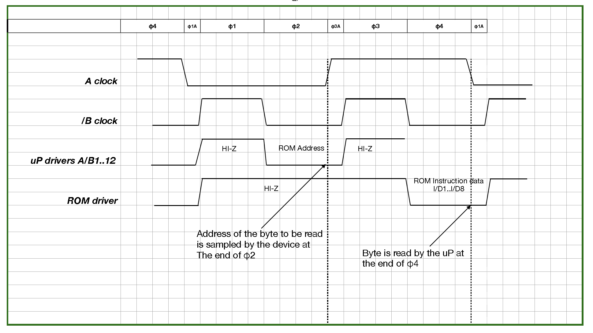
| φ# | A clock | /B clock | nb of ticks |
|---|---|---|---|
| φ1A | ↘ | (Low) | 1 |
| φ1 | Low | ↗ | 4 |
| φ2 | Low | ↘ | 4 |
| φ3A | ↗ | (Low) | 1 |
| φ3 | High | ↗ | 4 |
| φ4 | High | ↘ | 4 |
The ROM part of the A17 might potentially deliver one byte per cycle to the uP, (200KHz)
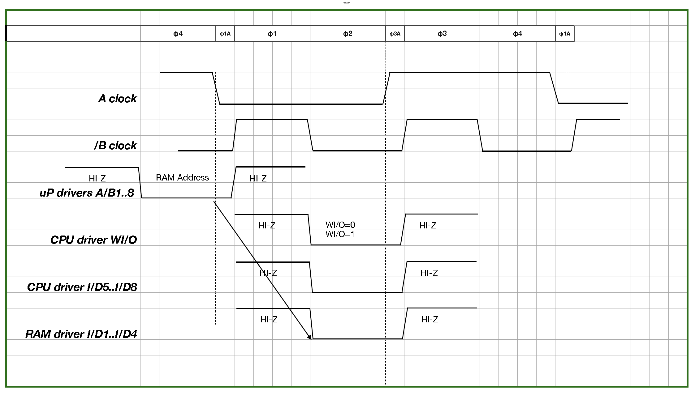
The data memory section (RAM) is addressed during φ4. In this circuit the state of the RRSEL during φ4, the internal code established during fabrication, and the A/B8 signal will establish if the RAM in the memory circuit is being accessed. Bot the A/B8 and RRSEL signals must match the internal code to select the RAM. The lower 7-bit of the address will then establish which 4-bit word is being accessed. The WI/O line will determine if the action to be performed is a read or a read and simultaneous write.
Depending on the version of the A17, those bits are internally set to 1 or 0. This configuration is made during fabrication. Of course, it cannot be modified later. This architecture allows the designers to map 2xA17xx's RAM, not requiring any glue logic.
We have already seen that determining if RRSEL=0 or 1 is complicated. So it is for A/B8, even worse.
For each cycle: The A17xx RAM subfunction samples the seven addresses lines A/B1..A/B7, plus RRSEL&A/B8, at the begining of φ1A. Then, if [RRSEL, A/B8] matches its internal configuration bits, the device will be activated. It will place the nibble at address A/B1..A/B7 on I/D1..I/D4 data bus for the duration of φ2+φ3A, so that the uP can sample them at the begining of φ3A.
In addition to this, WI/O is sampled by the device at the begining of φ3A. Depending on the value of WI/O, the nibble present on I/D5..I/D8 (placed there by the uP) is read simultaneously, and stored in the device.
The I/O section is triggered by the execution of an IOL instruction in the uP which causes the WI/O line to signal all I/O devices in the system that the next instruction byte contains a device identification (4-bit) and the specific command to be executed (4-bit). The IOL instruction, via the WI/O line, also tells the RAM to stay off the data bus so that the input/output data may be transmitted.
In an A17 component, the I/O subsection is identified by a number that is coded inside it. Possible values are 0, 2, 4, or 6. This values are not defined by pure accident: As a matter of fact, for example, a GPKD device (PPS4/2, anterior to the PPS4/2s components) #10788 can also been selected through the same mechanism. But for this chip there are only 3 straps, SC5, SC6, and SC7 that are compared to I/D5..7. The chip is only selected if straps match and I/D8 is at logic "true". Then 8 10788 can be separately selected in a design, without complexity. So, 0, 2, 4, 6 are the only free values that will avoid any confusion with other previous component, defined earlier.
This is an important remark that means that it is not enough to check I/D5&6 to determine if a given A17 is selected, but the whole nibble.
In an A17xx, the I/O subsystem is likely the most complicated part of the device that is to be understood (in order to be able to clone them). The most surprising thing is that the datasheet reads that this chip includes an input/output capability which allows the individual control of 16 one-bit I/O ports.
Individually controlled? Yes, this assertion is surprising enough by looking at the commands this subsystem can handle.
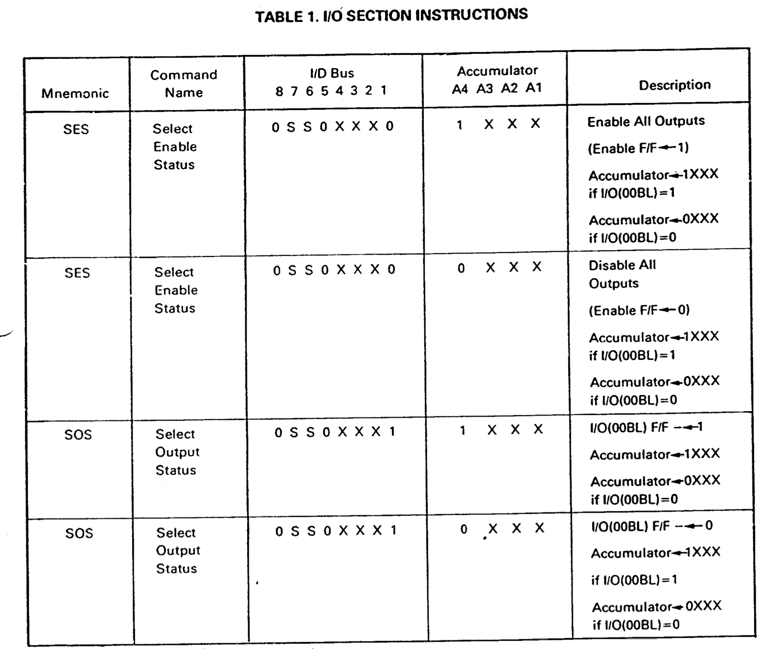
So, there are only 2 generic commands:
SES (Select Enable Status)SOS (Select Output Status)
It clearly reads that SES, while it gets an individual input value (with BL), it controls all the 16 outputs at once.
A4=0 ==> All outputs are disabled,
A4=1 ==> All outputs are enabled. SOS, on its side, will set the output whose the number corresponds to BL. What does all this mean?
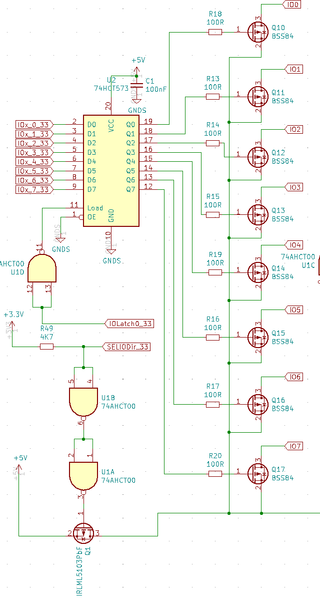
Before trying to deeply understand the atomic operations that an A17's IO section can perform and how, let us start by looking at the probable corresponding electronic circuit of this dynosauric (though magnificient) component. The best way is to look at what we've made for our clones. First, let us have a look at the simplified schematics for IOs:
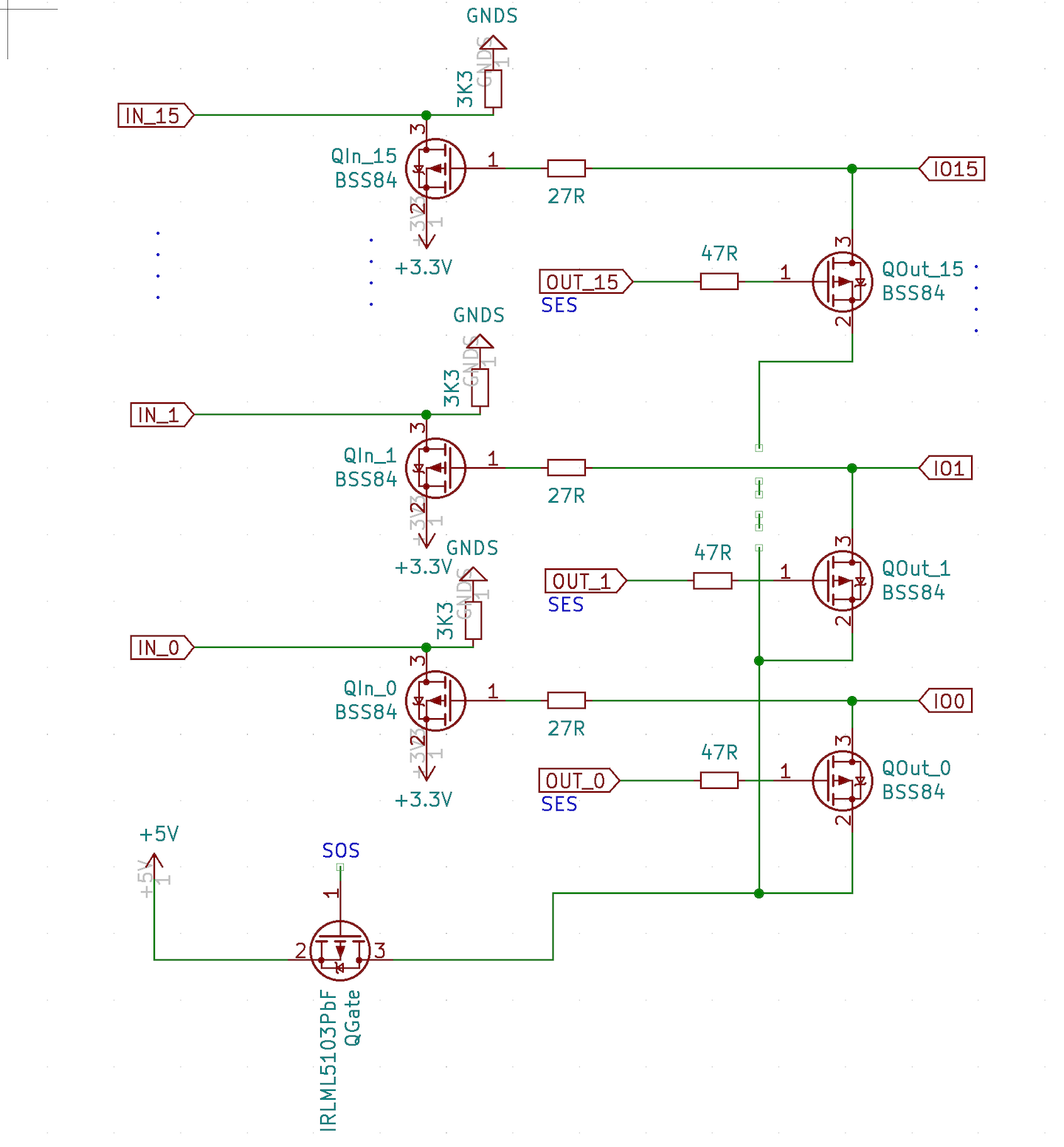
Have a particular attention to QGate. QGate will determine if all the outputs are Hi-Z, or deliver +5V, provided that QOut_x (for example, IO0) is on. So, for a given IOi, you have 3 MOSFETs involved. Example with IO0:
| QGate - control output | QOut_0 - set output value | QIn_0 - read input | IO pin |
|---|---|---|---|
| off | X | read ext. pin signal | value set by ext. circuitry |
| on | off | read ext. pin signal | value set by ext. circuitry |
| on | on | Internal read 5V | pin is forced to 5V |
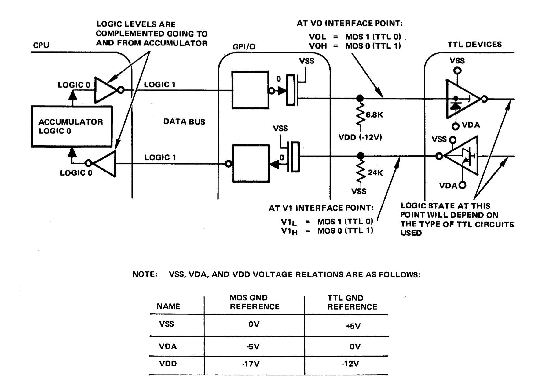
For your information, see below the picture that made us understand this principles. This is actually a drawing for GPIOs of PPS4/1, so it is a bit out of scope, since in PPS4/1 IOs are whether dedicated inputs or dedicated outputs, but not both. Nevertheless, this is what was missing in the PPS4/2 documentation to make one understand what was going on there.
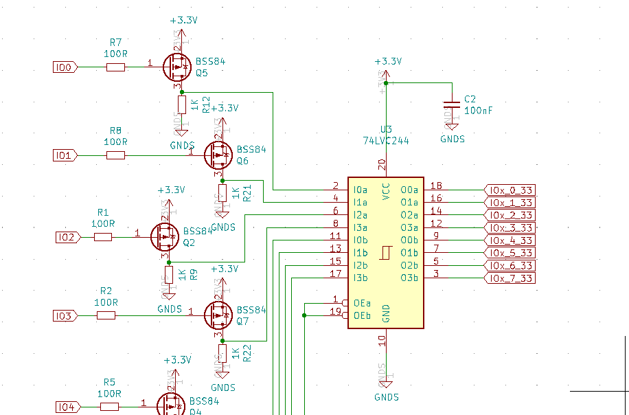
For your information, the next 2 figures will give you a detailled view of what we've develop for our clones:
To fully understand IOs timing you will need two pieces of information:
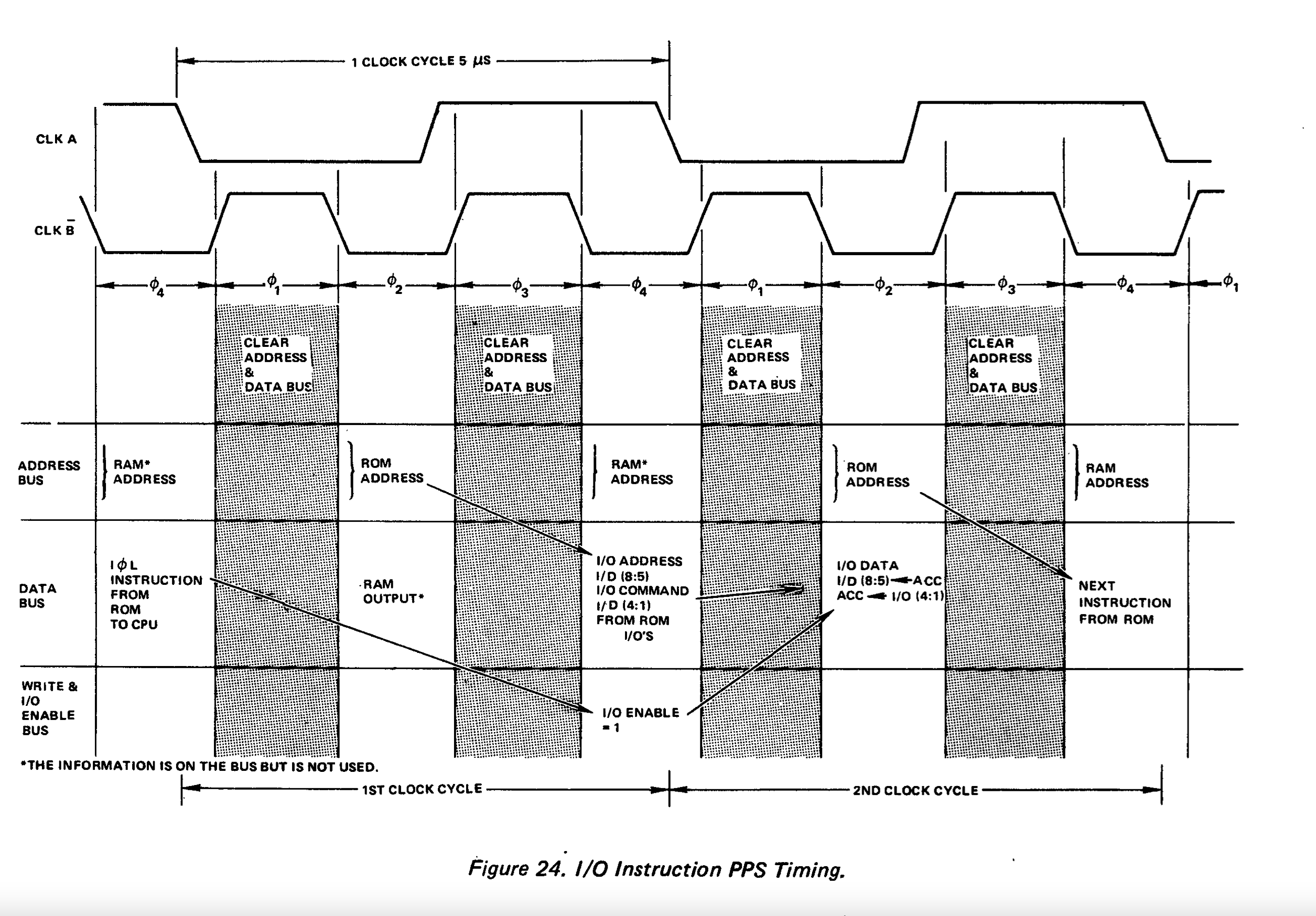
Typically on the figure above, it is marked (*) that RAM address read during φ4 is not used... Which is true in IO devices of the /1 generation, but wrong concerning the /2 generation, and among them the A17xx chip. Actually, This RAM address (only AB1..6) will hold the IO Port num of the current IOL execution. These discrepancies are perfectly understandable simply because /2 were still not even devised at the time the docs for /1 were printed. For the A17s, only AB1..4 are relevant since there are 16 IO ports. The documentation reads that AB5..6 must be set to 00. What happens if not, we don't know to be honest, but we think that they are not read at all by the A17s. They are probably "don't care" pins.
How is it managed from a coder point of view? Easy! IOL 0xhhll is the instruction, where hh contains the device ID, and ll the command. This functionality is common and identical for PPS4/1 and PPS4/2. But in the case of PPS4/2, prior to this instruction, the code must have set the adress register A/B to the number of the IO port. In PPS4/1, this address is only used for RAM access, thus it is (as specified in the doc) not used. Nevertheless, reading all these docs 50 years later, implies that it takes a while until you undertand that mess (which is nothing but History and evolution, eventually).
The timing is to be understood as follows:
SES or an SOS. Only 1 (whose ID=ID8..5) will stay active and handle the command. SES (ID1=0): This command will control QGate and determine if all 16 I/Os are enabled (powered by VSS (if corresponding IO is on) or floated. Powered when A4=1, floated otherwise. SOS (ID1=1): This command will individually control the state of a mos driver. The concerned IO number is identified by AB1..4. A4=1 ==> IO(BL)=1, A4=0 ==>IIO(BL)=0
A last piece of information about IOs of A17xx circuits: The documentation reads that at reset, the enable flip flop is set to 0 ensuring that all IOs are floated, but that the individual holding flip flops are not set automatically. This is not true! How do we know that? That is a funny story which costed us 2-ish weeks of lost in debugging. We recount it there.